The first principle of combinational logic is that a circuit must not contain feedback loops. No logic gate may have an output which could affect its input. The shortest way to explain why is just this: Feedback Is Memory.
If a combinational circuit contains any loops in its logical pathways, then it will be storing information in some form. This situation is sometimes glossed over a little bit in introductory courses, but this rule in combinational logic is also the foundation of the second main lesson of digital logic: sequential logic. Sequential logic circuits employ memory, also known as state, to allow sophisticated behavior which, unlike combinational logic, is time-dependent and influenced by past logic states which are no longer present. The relationship between these two is sufficiently confusing that with the advent of FPGA systems as a primary tool for logic labs, it is often glossed over or ignored altogether. Using the more hardware-centric capabilities of Verilog, we can explore some of the basic circuits which begin to exhibit state, and in so doing, nail down the often-confusing principles that dictate the behavior of sequential logic.
Let’s look at what I consider to be the foundational circuit of sequential logic, the keeper loop:

The keeper loop is something I didn’t actually see until almost a year after my first logic class, because it represents an intermediary step towards the circuit usually used for these purposes: the RS Latch. Simulating it in verilog is actually quite straightforward:
module bench;
  wire out, out_n;

  not x1(out, out_n);
  not x2(out_n, out);

  initial begin
    $dumpvars(0,bench);
    #5;
    $finish;
  end
endmodule
Verilog does not care that you are building a feedback loop, and it will simulate this circuit and show you that out and out_n both are unknown values in some way. Depending on your version of Verilog, this may either be expressed with the X state (value exists and is driven, but is unknown) or the Z state (value exists but is not driven, and the value is unknown).
There are two stable possibilities, however, which are not shown unless you set an initial condition of the system. They are that out_n is 1 and out is 0, or that out_n is 0 and out is 1. Either case will be the physical result of building this circuit on a bench, and knowing which one will happen depends on the internal resistances of the two inverters as they power on.
We can make a version of this circuit whose feedback can be switched on and off, however, which is how we arrive at the RS or “Reset/Set” latch. Here it is, in schematic and verilog:

module bench;
  reg r,s;
  wire out, out_n;

  nor x1(out,out_n,r);
  nor x2(out_n,out,s);

  initial begin
    $dumpvars(0,bench);
    #5;
    r=0;
    s=0;
    $5;
    r=1;
    #5;
    r=0;
    #5;
    s=1;
    #5;
    s=0;
    #5;
    $finish;
  end
endmodule
I’ve included a short set of test vectors so you can really see what’s happening. If I run it through Icarus Verilog and GTKWave I get this plot:
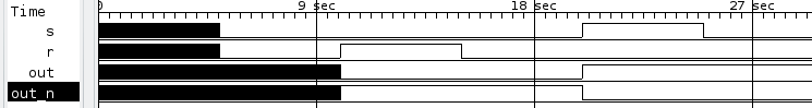
The black areas are places where the simulator does not know the value of the symbol in question, and in this case it is the X value. In the “hold” state of the latch, both inputs are zero, so the two NOR gates act like a keeper loop. As before, their internal value isn’t knowable. But thanks to the NOR gates, it is settable. At t=10, the input r is set high, causing a “reset” which sets out to 0 and out_n to 1. The latch holds on to that state afterwards, now acting like a keeper loop with a known state. A pulse on the input s has the opposite effect, showing that the circuit can be set to either of these two states by changing the values of its inputs.
After over 600 words, we are now able to show that this circuit can store and retrieve one bit of data. It also does so by a pretty awkward mechanism, but like with many things in engineering, building something that’s hard to use is easier than building something that’s easy to use.
A much more common memory circuit is the D Latch, and more common than that is the D Flip Flop, which is more complex, but sufficiently easy to use that it is the standard for synchronous memory systems. Next week we’ll look at two ways to make the D Flip Flop, with individual gates, using structural verilog, and with code that merely describes what it does, IE behavioral verilog.